
DIY and Pre-Assembled Eurorack Products
A Database And Planner:

Purchase Here
A Database And Planner:
Purchase Here
note: the power shown in this particular schematic is not the most up to date pwoer configuration RYO uses - we now recommend 72V 0.25A PTC resettable fuses not 10r resistors and 1N5818 Schottky diodes reverse biased to ground to lessen voltage droop across the rails.
also, we use an extra pair of decoupling caps now and when running a 5V regulator the decoupling cap setup we use has changed too. current schematics in the info repository on this site are currently being updated and hopefully kits will reflect these changes in the near future.
[also the gnd connection to the power header is conspicuously missing on that particular power-intro circuit above!] D:
Technically some of the stuff discussed so far was done a few years back as a proposed RYO module but abandoned as not suitable for a profit driven business. As a learning process though, it is ideal, so when a chance came to involve some people who could actually contribute useful input and would be enthusiatic and inspired by it as well as truly benefit it was a perfect moment to open the floor. as a result this caused the developemnt process to return to the more advanced parts of the basic design phase and good thing it did because there was still much to be done:
PART 3: DETAILED DESIGN AND FINALISATION PRE-PROTOTYPING
having shown the current proposed idea schematics it was time to start discussing everything that could possibly be thought of prior to breadboarding – this wiould allow a full BOM to be made for ordering breadboard/prototyping parts and agree on any undecided issues that would require changes or experimentation.– how big should the modules be – therefore dictating whether minipots would be used [decision was minipots too frail and wobbly, as well as resulting in finger-cramping poor ergonomy].
– how many/where/what colour leds should be used to indicate any inputs, outputs, delay times, gate lengths etc [decided on input signal present led and output led that would show delay presence as well as gate length].
– should the module generate its own 5V supply or derive it from the busboard [decided to include internal 5v gen so those with no 5v bus presence wouldnt be inconvenienced]
– testing of delay and gate length ranges are good – what size timing caps would be best [decided also to consider a switchable cap choice so each delay/length channel could have range switches]
– are the 5v/10v suitable voltages for the output options [are they needed? if so what for?]
[Within the A-100 usually any voltage beyond about +3V is treated as “high” (e.g. +5V, +8V, +10V, +12V will work) and will trigger an ADSR or any other module with a Gate or Clock input (e.g. trigger delay, sequencer, clock divider, clock sequencer).] from 0 V to +8 V for ADSRs; Trigger, Gate or Clock Signals typical voltage levels of 0/+5 V.
– a database of known clock/gate/trig issues that are due to reset/clock/midi issues is def a good idea, i.e. note voltage/spikes/slew/gnd issues to help those who might think they need this module but it wont help,
can post soltuions given in forums to save people time – that’ll make us popular as a rource and goto info source on clocks etc – to go in the back of the manual perhaps?
– Who was gonna do the breadboarding/CAD translation to get the experience under their belt and therefore plan discussions of talk through the early schematics and familiarise others with the necessary info.
its also worth mentioning that some of this process is eased by prior experience of being part of a commercial/industry design team – i specifically design to use as small a number of component values as possible so that:
a) it’s less complex a build.
b) it’s less complex kit to pack, check and therefore avoid mistakes etc.
c) it costs less when bulk ordering components from factories in mass production [one change in a resistor value could change the bom cost by hundreds or even thousands on major scale].
d) tolerances of components have less overall effect because they tend to balance out when there’s lots at the same tolerance.
e) it’s easier for humans to build [finding the right component takes less time the less dif ones there are], and, it’s easier for production pnp machines – cheaper the less reels have to be changed or the less different ones you use.
f) shipping requires less packaging from component source and kit packaging needs - less bags etc.
g) there’s less colour codes etc for a beginner to learn.
h) speeds up and reduces risk of placing a wrong value component the simpler you keep things.
[
ok thats all the reasons i can think of for now but i’m sure there’s more
]
as you can see, therefore there’s a good chance you may find some things can be easily built of existing parts you have – some r, c and d values/types are ridiculously common in all electronics – way more than most others, fundamentally though there’s always gonna be things you havent come across before or you dont have any of left because you only had one since they aint used much…
also certain components just plain cant be substituted – for example although this design makes it possible to change values of resistors in the output buffers to get the same amplification using a number of different combos, it’s not possible to substitute the 100uf electrolytic cap on the 5v power converter – that’s just straight out strictly required according to the datasheet, and if you aint got one then you buyin one! [most of the components in this thing cost like 0.1c each, it’s only pots and the power cable that are around the coupla $ mark]
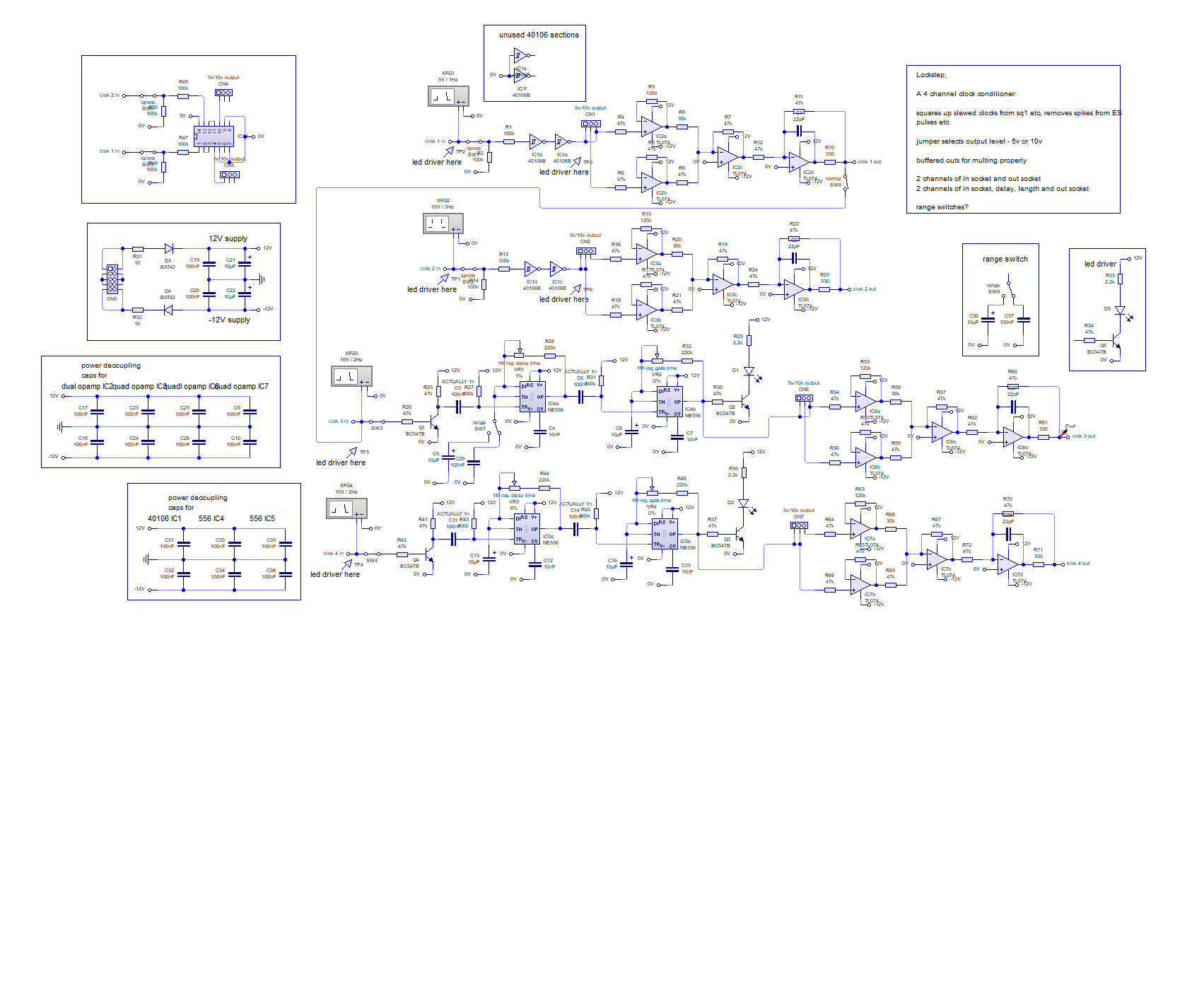
THE UNNAMED GROUP OF PEOPLE'S 'LOCKKSTEP' CLOCK CONDITIONING MODULE
ideas [to be] discussed:
- check if this module exists - has something been missed? can we improve? can we make it as good even? etc.
[think were ok - checked mod grid once, need 2nd onion]
people use a Doepfer A-160-2, amplifier like the A-183-3 (weak clock signal), an active buffer (ground issues) or a trigger modifier like the A-162 (slewed or otherwise invalid clock signal),
- what modules have clock/trig issues? will it fix em? can it be made to fix em if not?
[search mod wiggler/google for modules and units with clock/gate/trig issues;
- go through mod grid identifying things using clocks or gates with same potential issues - look deep!
so far:sq1 slewed clocks, es pulses spikes, marbles when supply voltage stabilizes slowly to its target voltage,
something that depends on which PSU you use, where your module is located, and how other modules on the bus board behave,
PNW seems to be one that doesn’t like to be slaved, something with Rene?,
slaved Metropolis often needs a dedicated reset signal that is different from (earlier than) the reset bus all other slaved seqs get].
- not mini pots
- leds on other ins n outs to show clock/trig signal present/length?
- what colour leds mean what? should dif colours display dif gate/trig length?
- will it goes as smol as 4-6hp [is this wise? too crammed? ...[def wont fit 4hp!]
- 5v internal generation ok?
- need to see if the delay and length times are a good range
- are the 5v/10v suitable voltages for the output options [are they needed?if so what for?]
[Within the A-100 usually any voltage beyond about +3V is treated as "high" (e.g. +5V, +8V, +10V, +12V will work) and will trigger an ADSR or any other module with a Gate or Clock input (e.g. trigger delay, sequencer, clock divider, clock sequencer).]
- from 0 V to +8 V for ADSRs; Trigger, Gate or Clock Signals typical voltage levels of 0/+5 V.
- a database of known clock/gate/trig issues that are due to reset/clock/midi issues, i.e. not voltage/spikes/slew/gnd issues to help those who might think they need this module but it wont help,
can post soltuions given in forums to save people time - that'll make us popular as a resource and goto info source on clocks etc - to go in the back of the manual perhaps?!
*************
BOM for 'LOCKSTEP'
-----------------------------------------------------------------------------------------------------
resistors:
- r 1,2,9,13,14,27,31,43,45 100k 8 all the same pretty much...
- r 4,5,6,7,9,11,12,16,17,18,19,21,
22,24,25,26,30,37,41,42,54,56,
57,59,60,62,64,66,67,69,70,72 47k 32 all the same pretty much...
- r 8,20,58,68 30k 4 all the same pretty much...
- r 51,52 10r 2 all the same pretty much...
- r 3,15,53,63 120k 4 all the same pretty much...
- r 10,23,61,71 330r 4 all the same pretty much...
- r 28,32,44,46 220k 4 all the same pretty much...
- r 29,36 2.2k 2 all the same pretty much...
capacitors:
- c 9,10,17,18,19,20,23,24,25,26,
31,32,33,34,35,36 100n 17 ceramic c0g 2.5mm or equiv
- c 1,2,27,28 22pf 4 ceramic c0g 2.5mm or equiv
- c 3,6,11,14 1n 4 ceramic c0g 2.5mm or equiv
- c 4,5,7,8,12,13,15,16 10n 8 ceramic c0g 2.5mm or equiv
- c 21,22 10uF 2 electrolytic, 25v, 2mm pin pitch, 5mm dia, 5mm height
transistors:
- 1,2,3,4 BC457B 4 to-92 packacge
diodes:
- d 1,2 amber? 2 LED, 3mm
- d 3,4 SB130 2 or 1N5818, schottky power
integrated circuits:
- ic 1 40106 1 cd4xxxb cmos logic hexinverter w/ schmitt trigger
- ic 2,3,6,7 TL074 4 opamp
- ic 4,5 NE556 2 dual timer
Hardware:
- p 1,2,3,4 1M log 4 rotary pots
___
- j 8 x jacks 3.5mm mono, un-switched - like PJ301BM or kobicon/clone [not too important for bb]
___
[for 5v supply if not taken off bench psu]
- vr x lm2391 1 5v fixed voltage regulator, to92 package
- c x 100n 1 ceramic c0g 2.5mm or equiv
- c x 100uF 1 electrolytic, 25v, 2mm pin pitch, 5mm dia, 5mm height
***********
not needed for breadboarding - only for pcb
connectors:
___
- 1 x 10pin 10pin boxed power header
- cn 1,2,6,7 3pin 4 3pin jumper header
- cn 1,2,6,7 2pin 4 2 socket insulated jumper
- is 1,2,3,4,5,6,7 14pin 7 ic sockets, 14pin
___
- cbl x 1 10-16pin eurorack power cable
___
- also will be needed: knobs, screws, pcb, faceplate,
STEP 4: A NEAR FINISHED SCHEMATIC / PROTOTYPING CONT.
after some discussion here’s the current state of affairs ready to be breadboarded - this is where the project last stalled and still, therefore, awaits testing, pcb routing, further testing and finishing off:

If this inspires or educates anyone in a ny useful way please feel free to do what you wish with all this and please do keep us in the loop - we'd love to hear of your successes and discoveries and any other cool experiences that may have resulted - go forth and have fun!